Machine Recycling Discussion and Moderated Newsgroup > Separate Parts
> Knobs and Handles
> West
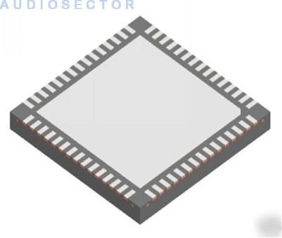
> CDCE72010 clock synchronizer cleaner distrib. 10 out X2
CDCE72010 clock synchronizer cleaner distrib. 10 out X2
10 Output High Performance Clock Synchronizer,
Jitter Cleaner, and Distributor
High Performance LVPECL, LVDS, LVCMOS PLL Clock Synchronizer
Two Reference Clock Inputs (Primary and Secondary Clock) for Redundancy Support with Manual or Automatic Selection
Accepts Two Differential Input (LVPECL or LVDS) References up to 500MHz (or Two LVCMOS Inputs up to 250MHz) as PLL Reference
VCXO_IN Clock is Synchronized to One of Two Reference Clocks
VCXO_IN Frequencies up to 1.5GHz (LVPECL)
800Mhz for LVDS and 250MHz for LVCMOS Level Signaling
Outputs Can be a Combination of LVPECL, LVDS, and LVCMOS (Up to 10 Differential LVPECL or LVDS Outputs or up to 20 LVCMOS Outputs), Output 9 can be Converted to an Auxiliary Input as a 2nd VC(X)O.
Output Divider is Selectable to Divide by 1, 2, 3, 4, 5, 6, 8, 10, 12, 16, 18, 20, 24, 28, 30, 32, 36, 40, 42, 48, 50, 56, 60, 64, 70, or 80 On Each Output Individually up to Eight Dividers. (Except for Output 0 and 9, Output 0 Follows Output 1 Divider and Output 9 Follows Output 8 Divider)
SPI Controllable Device Setting
Individual Output Enable Control via SPI Interface
Integrated On-Chip Non-Volatile Memory (EEPROM) to Store Settings without the Need to Apply High Voltage to the Device
Optional Configuration Pins to Select Between Two Default Settings Stored in EEPROM
Efficient Jitter Cleaning from Low PLL Loop Bandwidth
Programmable Phase Offset (Input Reference to Outputs)
Wide Charge-Pump Current Range From 200 A to 3mA
Dedicated Charge-Pump Supply for Wide Tuning Voltage Range VCOs
Presets Charge-Pump to VCC_CP/2 for Fast Center-Frequency Setting of VC(X)O, Controlled Via the SPI Bus
SERDES Startup Mode (Depending on VCXO Range)
RESET or HOLD Input Pin to Serve as Reset or Hold Functions